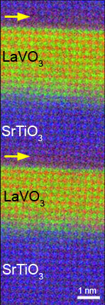
 Atomic-resolution EELS chemical composition map taken on the Nion UltraSTEM 100 microscope. V = red, La = green, Ti = blue. Yellow arrows point to purple bands showing V/Ti intermixing. This 128x375 pixel spectrum-image was taken at 10ms/pix (~15 min total acquisition) with no drift compensation. (Courtesy L. Fitting-Kourkoutis & D. Muller) 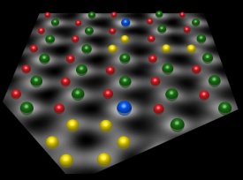 ADF image of monolayer boron nitride containing atomic substitutions. Quantitative analysis of the image produced a detailed atomic model, which is shown superposed on the image. Boron atoms are shown red, carbons atoms yellow, nitrogen atoms green and oxygen atoms blue. Graphic courtesy Tim Pennycook, ORNL & Vanderbilt U. |
Nion microscopes have been designed from the “ground up”. This has allowed them to avoid having any “historical design baggage” that is typically found in other electron microscopes. The result is an integrated performance second to none. Nion microscopes have many features not found in other instruments, with benefits that increase productivity and provide opportunities for new kinds of experiments:
|
Nion's Ultra-High Energy Resolution Monochromated EELS-STEM combines our monochromator and spectrometer to achieve energy resolutions of < 6 meV (at 60kV). It offers high energy dispersion up to 0.1 meV/channel (at 60 kV), and a large energy range of up to 1 keV at 60 kV and beyond 2 keV at 200 kV. Energy drift is less than 5 meV / minute, providing excellent long-term stability.
The HERMES can be built around either beam source used in UltraSTEM™ systems, either Nion's 200 kV CFEG or the VG 100 kV gun.
This electron microscope extends the range of operating voltages of the Nion microscopes to 200 kV. Its column is similar to the UltraSTEM™ 100, but it uses a new, high brightness/high stability cold field emission gun developed by Nion.
The gun features several new design elements that allow operation at lower voltages at performance levels similar to guns optimized to function only at the lower voltage.
The higher operating voltage gives:
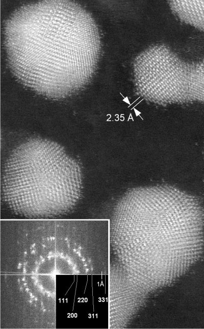
HAADF image of multiply twinned gold crystal particles (800x1200 pixel sub-area of a 2048x2048 image is shown). UltraSTEM200™ operating at 200 kV.
Many fine spacings in the particles and well resolved single atoms lying next to the particles can be seen.
The insert shows the Fourier transform of the whole image.
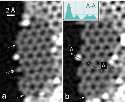 Medium angle annular dark field (MAADF) images of the edge of graphene, taken 2 minutes apart. Note the extensive rearrangement that occurred at the edge, and the heavier adatom (probably Al) dangling off the edge. Single arrows in4 (a) show five-fold C rings, the double arrow shows a single atom of C dangling off the edge. Nion UltraSTEM™ 100, 60 keV. (Krivanek et al., Ultramicroscopy 110 (2010) 935-945) |
The UltraSTEM™ 100 is a high-performance dedicated scanning-transmission electron microscope (STEM) with many unique features. Its flexible column provides < 1 Å resolution imaging as well as rapid nanoanalysis with an atom-sized electron probe containing > 0.5 nA of current, and efficient coupling into a variety of detectors. It can also produce high-quality diffraction patterns and even CTEM images. The UltraSTEM™ has produced atomic-resolution elemental maps in less than a minute (see results). This promises to lead to a new era in electron microscopy in which atomic-resolution elemental maps become a powerful addition to the range of available microscopy techniques. It has also produced unsurpassed images of graphene and similar light-Z materials, while operating at 60 keV, below the knock threshold for C and other light atoms. The principal design elements of the UltraSTEM that have made this advance possible are:
Many of these features are unique to the Nion microscope. A full description of the microscope was published in Ultramicroscopy. |
Nion is a small and responsive company whose scientists and engineers are deeply knowledgeable about electron microscopes and very interested in pursuing new applications. Our UltraSTEM microscopes are completely modular; all the modules of the microscope column use the same exact mating surface. They can therefore be stacked in almost any sequence and total number. The vacuum system, the electronics, and the detector column are also modular. This means that the column can be reconfigured in many different and unique configurations.
The service of Nion microscopes is based on four principles: